If the CCD were operating in a true
on-off mode, such low amplitudes would have serious aliasing, or cell-to-cell
disŁtortion components. Instead the CCD opŁerates as a very wide dynamic range
linear sensor, where each of its 256 cells is able to yield 40 dB dynamic
range, between the maximum illumination and the averaged noise. One hundred discrete
illumination levels can be detected, with 50% or better certainty, and defined
as signals from any of these cells. When cell-to-cell uniformity, scattering
and exciter flux uniformity are considered, these defined points or levels are
reduced to 50. A linear phase-interpoŁlation filter is designed for an overlap
of 4 to 5 cells, so that the final transition region presented to the sliced
comparator is made from a statistical average of 2 cells, yielding 60 to 70% of
the sample; 2 more yielding 20 to 30% and the remaining adjacent cells
contributing a small amount to the sample. When all of these are averaged, 6 dB
for the in-phase optical phenomenon and 3 dB for statistical noise, the
resulting sample at the transition can resolve about 200 levels. The transition
rise time is about one fourth that of the electrically scaled 12-kHz resŁolution.
However, the entire transition reŁgion can still modulate back and forth at the
12-kHz rate, as the sideband frequencies are small when compared to the roughly 1-MHz cutoff of the
phase-interŁpolation filter. In sweeping back and forth, the transition slice
region has about 1/200 of cell-to-cell alias ripple, an amount well below the
intrinsic electronic noise. Thus the best-case incremental resolution would be:
4 cells X 13 µm/200 points = 260 nm
This aliasing or incremental
cell-to-cell noise is well below the 1 to 4 µm scaled electronic noise,
achieving 46 dB dynamic range. These numbers convert to pulse differential
times, giving a 2.5 ns electrical resolution. Such accuracies have necessiŁtated
an unorthodox logic design, calling for very careful board layout, to prevent
random crosstalk spikes. This careful control of clock jitter and its resulting
low noise at the CCD output allows scan reading down to film grain dimensions.
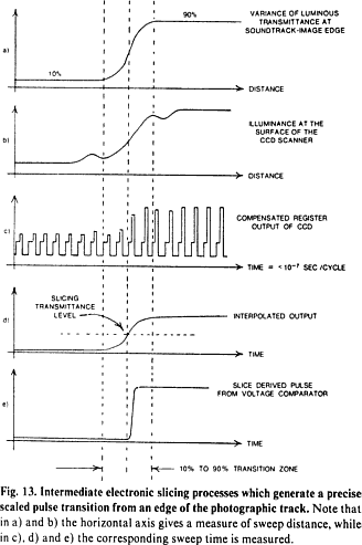
Cell Interpolation and Pulse Generation.
The ideal 1 to 4 µm transition boundary almost doubles at
the CCD beŁcause of scattering, reflections and objecŁtive MTF. The multilevel
average signal from the cells
scanned in this region is presented as a series of clocked cell pulses to a
low-pass filter (Fig. 13c). This filter is tailored with a ripple function in
time, which matches and complements the proŁjected optical transmission
function in space. This arrangement permits many cells to be interrogated, yet
still to convert into pulses very narrow boundaries, which almost clash.
Without this technique, high-modulation noise would result as a tradeoff from
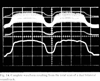
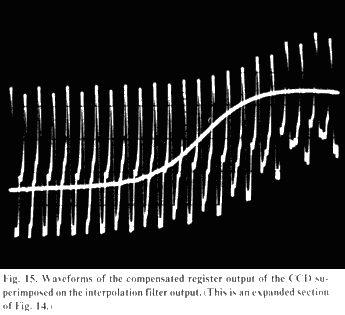
eliminating pulse crowding dropout noise effects at high modulation. Figure 15
is an expanded section of Fig. 14. It shows the clock cell pulses (Fig. 13c)
superimposed with the interpolation filter output (Fig. 13d). In practice, once
the optics and filter match occur, the electrical transition appears as near Gaussian.
The inflection point of greatest slope then coincides with 50% minimum to
maximum transmittance and also with the correctly scaled soundtrack object
image size. This optimization occurs simultaneously for pulse crowding,
modulation noise and cross-modulation axis shift. Additionally, the highest
width modulation at short wavelengths also occurs at this 50% point, yielding the
maximum high frequency output upon PWM conversion.